
PCB analysis.
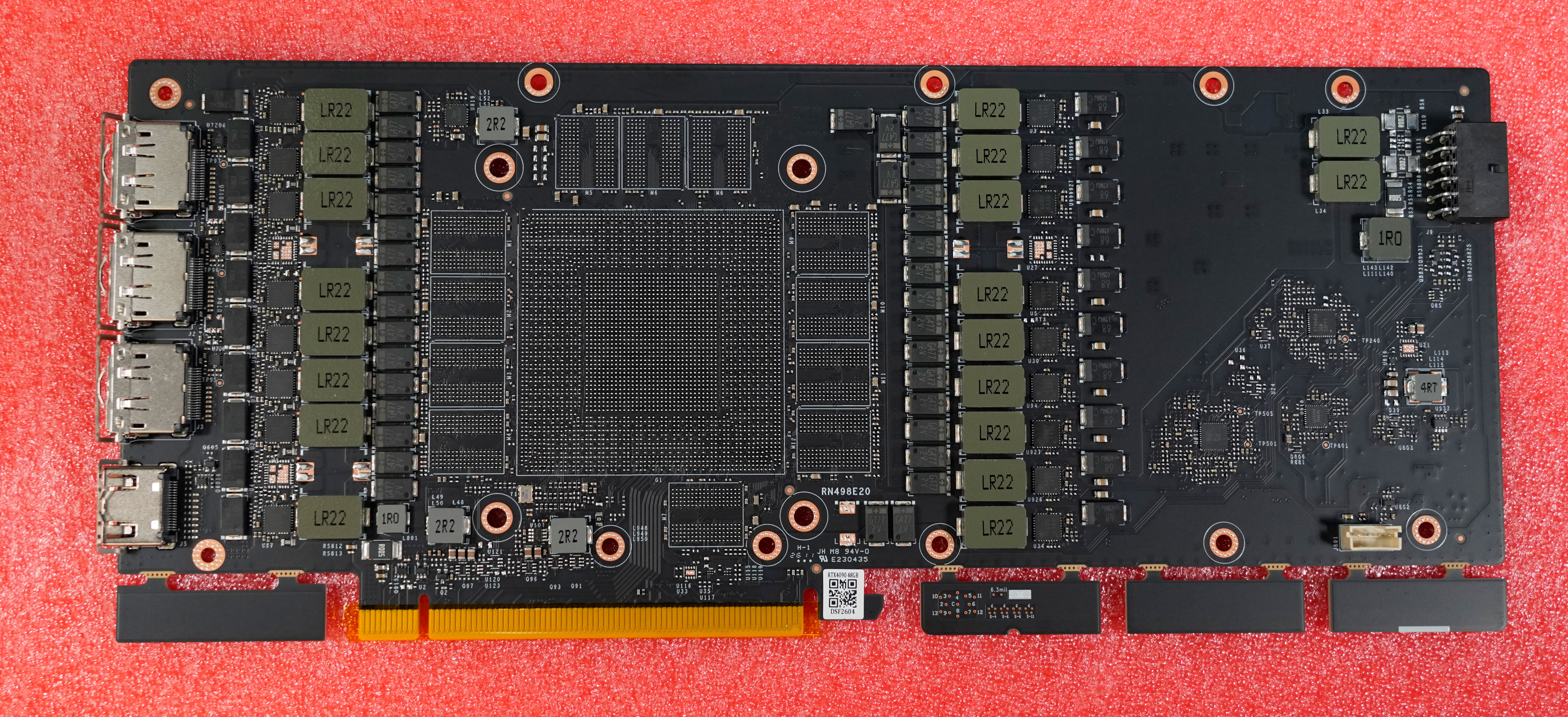
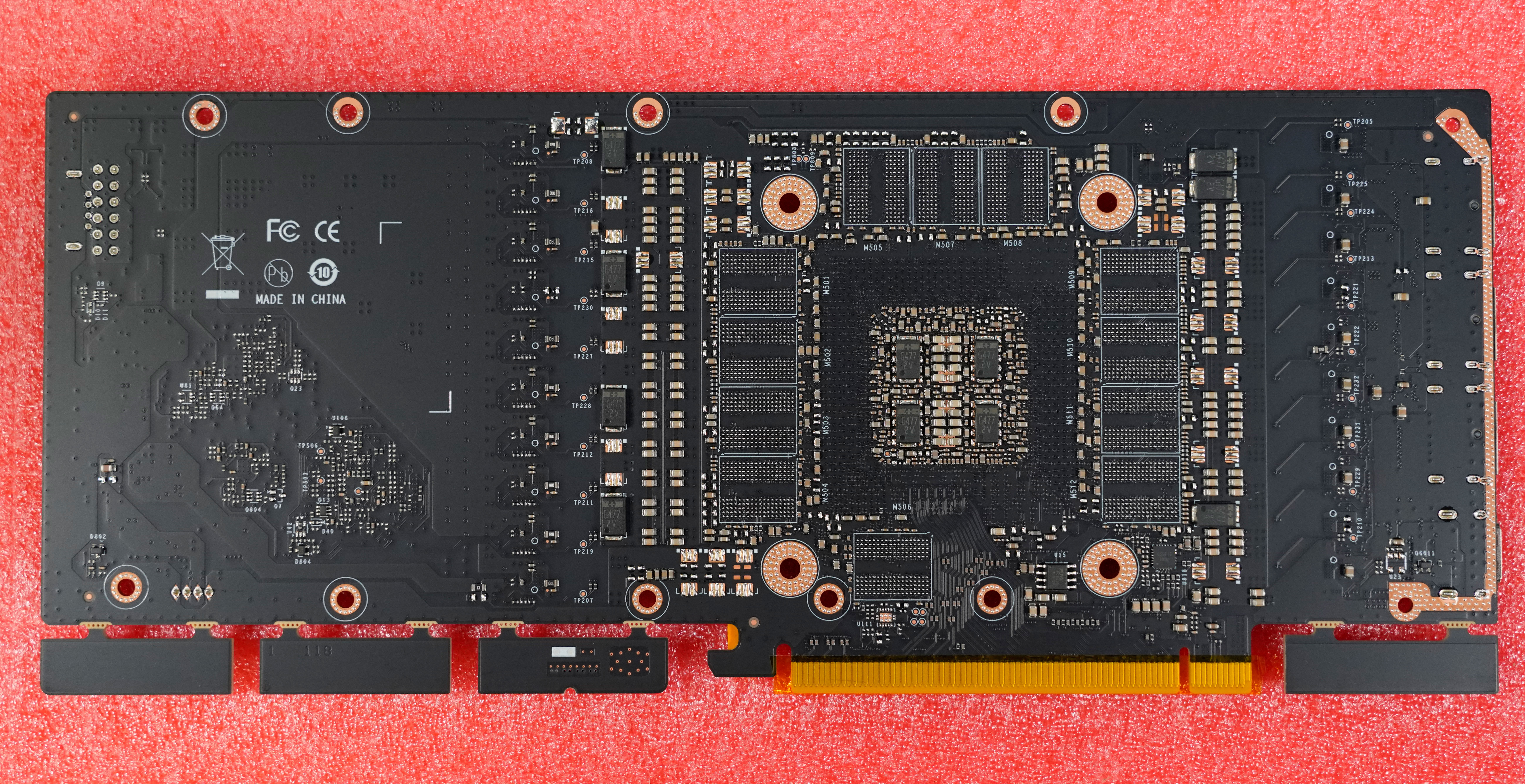
Component map
Hover (or tap) a row to highlight where the part lives on the board.
| Tag | Component | What it does | Side |
|---|---|---|---|
| A | Memory module pads | GDDR6X solder pads in clamshell mode. Twelve modules on the front pair with twelve on the rear to reach the 48GB total. Clamshell mode refers to Micron's design specification where chips can share the same data and address lanes, and the GPU can select which chip it's talking to billions of times per second (GHz speeds). | Front · Rear |
| B | Memory power stage (1.35V) | Four-phase power stage delivering 1.35V to the GDDR6X memory rails with an overkill 220A power budget. | Front |
| C | vCore power stage (1.0V) | Thirteen-phase core power stage delivering 450 W to the GPU core. Thermally efficient, low exposure to component failure, 40% overhead with 715A power budget. | Front |
| D | 12VHPWR connector | 450 W power input connector that feeds vCore and vMem. | Front |
| E | Fan connector | Header for the dual-bearing turbo blower fan. | Front |
| F | VBIOS chip | SPI flash that stores the NVIDIA FALCON GPU firmware (clock tables, power limits, memory topology). Reflashed during the 48GB conversion so the controller knows about the doubled memory. | Rear |
| G | 3× DisplayPort | Three DisplayPort 1.4 outputs in the bracket-side I/O stack. | Front |
| H | 1× HDMI | One HDMI 2.1 output alongside the DisplayPort stack. | Front |
| I | PCIe 4.0 ×16 connector | The card edge connector that plugs into the motherboard. | Front · Rear |
| J | Smoothing capacitor banks | Higher-density MLCC and expensive tantalum capacitors sitting around the GPU and memory package on both sides of the PCB. They handle the sub-microsecond load transients a modern GPU generates so the core and memory rails stay stable under spike loads. | Front · Rear |
| K | Break-away tabs | Manufacturing tabs used to hold the PCB during rework. They snap away cleanly after the card is built. | Front · Rear |
| L | Current sensing resistors | Sub-milliohm shunts the VRM controller reads to monitor GPU power draw under load and feed telemetry back to the driver. | Front |
| M | GPU core pads | AD102 GPU core BGA pads. Over 3,000 solder balls at 0.5 mm pitch must reflow perfectly for the GPU to even turn on. | Front |
Upgrade process
From the moment your card arrives at the shop to the day it ships back.
Remove GPU core and memory modules
Using industrial BGA rework equipment, the AD102-300-A1 core and the 12 stock GDDR6X memory modules are de-soldered from your original PCB. Each component is cleaned and inspected before moving on.
Reball BGA, validate modules, prepare PCB
The BGA pads on the GPU core and on every memory module are carefully prepared and reballed with fresh solder spheres. Each module is functionally validated before assembly, and the new Gen 3 PCB bga pads are prepped and cleaned for bga rework.
Attach memory modules to a different PCB
The original AD102-300-A1 core, the 12 original GDDR6X modules, and 12 additional GDDR6X modules for the rear-side clamshell are soldered onto the new 48GB-capable Gen 3 PCB.
